Real-Time Order Tracking
Get full visibility of your orders from confirmation to delivery.

Driven by the global industry shift toward clean energy transition, electric mobility, and sub-nanometer chip architectures, high-tech manufacturing is undergoing a dramatic evolution: success no longer depends on commercial chemical supply alone, but on securing ultra-high-purity advanced materials engineered for absolute batch-to-batch consistency. To support this demand, our Advanced Materials portfolio delivers a specialized B2B chemical sourcing and custom synthesis contract manufacturing network designed specifically for the next-generation requirements of solar & photovoltaic wet chemical processing, battery active energy storage materials, and semiconductor chemical fabrication. Built to satisfy strict battery grade, electronic grade, and ultra-high-purity (EL, UP, UPSS, UPSSS) chemical specifications, our multi-tier vertical spans ultra-pure wet processing acids and bases, specialized silicon dopants, and electronic-grade solvents to organometallic ALD/CVD precursors, CMP polishing slurries, high-purity substrates, and photolithography etch chemicals. Whether supplying high-capacity cathode active material precursors, anode materials, electrolyte salts (LiPF6), and specialty battery binders for energy storage systems, or delivering sub-nanometer-ready semiconductor precursors and photovoltaic cell wet-chemical streams, we empower global technology innovators to scale rapidly with verified, resilient, and purity-certified supply chain solutions.
Typical first response within 24 hours.


.e9dec10a.svg)



100% guarantee on the quality of chemicals with a robust 3-step quality inspection process
Capabilities for producing APIs and Intermediates in controlled quantities tailored to your needs.
Cutting-edge research and development to improve process efficiency during manufacturing
Get full visibility of your orders from confirmation to delivery.
From lab-scale testing to pilot-scale production to finished formulations and regulatory support, our CRO services are designed to streamline your journey to market with precision and expertise.
From lab-scale testing to pilot-scale production to finished formulations and regulatory support, our CRO services are designed to streamline your journey to market with precision and expertise.
Category : Advanced Substrates, Crystals & Quantum Materials
Sub-Category : Thermoelectric & Phase-Change Materials
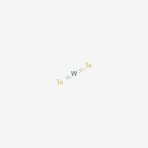
Description : We supply high-purity Tungsten Ditelluride (CAS No: 12067-76-4) to help technological breakthroughs across the international quantum computing, topological spintronics, non-saturating magnetoresistive sensing, optoelectronic switching, and solid-state energy harvesting markets. Recognised by international material scientists as tungsten(IV) telluride and identified across global chemical supply chains as tungsten telluride, this layered transition metal dichalcogenide (TMD) adopts an orthorhombic distorted octahedral structure (T'd-WTe₂, space group Pmn2_1. Exhibiting extreme non-saturating magnetoresistance (up to 13 million % at low temperatures), high carrier mobility, and non-trivial Type-II Weyl semimetal topological states, the material facilitates dissipationless electronic transport and non-linear quantum Hall phenomena. Having these rare quantum traits makes this unique crystal the leading choice for topological qubit interconnects, cryogenic magnetic field sensors, ultrafast broadband photodetectors, and thermoelectric energy conversion arrays. As global microelectronics markets push past conventional silicon limits, processing plants are changing their sourcing methods. Advanced materials factories are upgrading production lines by switching exclusively to our strictly controlled 3N (99.9%) to 5N electronic purity grades to secure optimal electron movement and eliminate structural lattice defects. Quantum foundries and device developers partner with us as their certified global tungsten (IV) telluride supplier to protect their production runs from material failures and cross-border shipping delays. Selecting us as your trusted tungsten ditelluride supplier guarantees an advanced material providing uniform layer-by-layer lattice matching and structural consistency during high-speed chemical vapour deposition (CVD), molecular beam epitaxy (MBE), flux crystal growth, and magnetron sputtering. Technical teams can verify our strict material metrics by downloading our batch-specific Tungsten Ditelluride COA and compliance documentation, which guarantees exact stoichiometric control, minimal trace-metal impurities, and consistent flake or powder dimensions. Get to our official telluride tungsten TDS sheets ensures complete compliance with global standards, including European REACH registration, RoHS directives, and ISO 9001 quality rules. Partnering with us as your preferred tungsten ditelluride supplier to lock in raw material reserves and scale your advanced product manufacturing lines, bypassing geopolitics supply chain instabilities
Category : Advanced Substrates, Crystals & Quantum Materials
Sub-Category : Thermoelectric & Phase-Change Materials
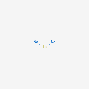
Description : We supply high-purity Sodium Telluride (CAS No: 12034-41-2) to drive technological breakthroughs across the internationally even developing organic chemical synthesis, specialised semiconductor doping, thermoelectric material research, photo-cathode manufacturing, and quantum materials sectors. Known to international synthetic chemists as disodium telluride and recognized across chemical supply chains as sodium monotelluride, this alkali metal chalcogenide crystal adopts an anti-fluorite cubic structure (Fm3m). Functioning as a powerful water-soluble nucleophilic tellurating reagent, it plays a vital role in introducing tellurium atoms into organic substrates to yield organotellurium intermediates, dialkyl tellurides, and specialized tellurium-containing polymers. Having these versatile reactivity traits makes this unique compound the premier choice for preparing advanced phase-change memory precursors, chalcogenide thermoelectric alloys, alkali photocathodes for particle accelerators, and specialised optoelectronic matrices. As global high-tech industries demand cleaner synthetic pathways and precise stoichiometry control, processing plants are upgrading their production lines by switching exclusively to our strictly controlled 3N (99.9%) purity grade to secure optimal reactivity and eliminate material flaws. Fine chemical producers and electronic device developers partner with us as their certified global disodium telluride supplier to protect their production runs from synthesis failures and cross-border shipping delays. Selecting us as your trusted sodium monotelluride supplier guarantees an advanced reagent providing reliable solubility and uniform reaction kinetics during organic telluration, liquid-ammonia synthesis, and chemical deposition processes. Technical teams can verify our strict material metrics by downloading our batch-specific Sodium Telluride COA documentation, which guarantees exact chemical purity, minimal trace-metal impurities, and controlled moisture limits. Accessing our official Sodium Telluride NaTe TDS sheets ensures complete compliance with global standards, including European REACH registration, RoHS directives, and ISO 9001 quality rules. Partner with us as your preferred Sodium Telluride supplier to lock in raw material reserves and scale your advanced manufacturing lines.
Category : Advanced Substrates, Crystals & Quantum Materials
Sub-Category : Thermoelectric & Phase-Change Materials
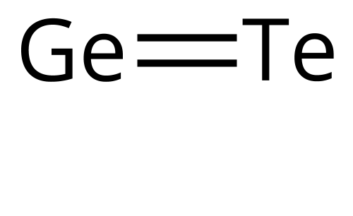
Description : We supply high-purity Germanium Telluride (chemical compound of <a href="https://en.wikipedia.org/wiki/Germanium" rel="noopener noreferrer" target="_blank">germanium</a> and <a href="https://en.wikipedia.org/wiki/Tellurium" rel="noopener noreferrer" target="_blank">tellurium</a> and is a component of <a href="https://en.wikipedia.org/wiki/Chalcogenide_glass" rel="noopener noreferrer" target="_blank">chalcogenide glass</a>) to power technological breakthroughs across the international non-volatile memory, thermoelectric power generation, ferroelectric spintronics, optoelectronic, and photonic switching markets. Known to international material scientists as germanium monotelluride and recognised across chemical supply chains as germanium(II) telluride, germanous telluride this IV-VI narrow-bandgap semiconductor crystal undergoes a reversible, fast phase transition between an amorphous structural state and a crystalline rhombohedral lattice (R3m). Exhibiting high electrical conductivity, strong ferroelectric polarisation, large spin-orbit coupling, and an optimal thermoelectric figure of merit (ZT' > 1.8 when alloyed near 700 K), the material serves as an essential component for phase-change random-access memory (PCRAM), solid-state energy harvesters, neuromorphic computing arrays, and active photonic devices. As global semiconductor foundries transition away from conventional silicon scaling limits, processing facilities are upgrading production lines by switching to our strictly controlled 5N (99.999%) to 5N5 (99.9995%) purity grades to secure optimal electron movement and eliminate phase-transition material flaws. Microelectronic foundries partner with us as their certified global germanium monotelluride supplier to protect their production runs from material failures and cross-border shipping delays. Selecting us as your trusted, germanous telluride supplier guarantees an advanced material providing uniform layer-by-layer lattice matching and structural consistency during high-speed chemical vapour deposition (CVD), molecular beam epitaxy (MBE), thermal evaporation, and magnetron sputtering. Technical teams can verify our strict material metrics by downloading our batch-specific Germanium Telluride COA and other documentation, which guarantees exact stoichiometric control, minimal trace-metal impurities, and consistent particle size distributions. Accessing our official (GeTe) TDS sheets ensures complete compliance with global standards, including European REACH registration, RoHS directives, and ISO 9001 quality rules. Partner with us as your preferred Germanium Telluride supplier to lock in raw material reserves and scale your advanced manufacturing lines.
Category : Advanced Substrates, Crystals & Quantum Materials
Sub-Category : Thermoelectric & Phase-Change Materials
Description : Stannous selenide is the most efficient <a href="https://en.wikipedia.org/wiki/Thermoelectric_materials" rel="noopener noreferrer" target="_blank">thermoelectric </a>material. We supply high-purity tin selenide (CAS No: 1315-06-0tin selenide) to drive technological breakthroughs across the international thermoelectric energy harvesting, thin-film photovoltaics, optoelectronic sensing, phase-change memory, and solid-state energy storage markets. Known to international material scientists as tin monoselenide and recognised across chemical supply chains as tin(I) selenide, this IV-VI binary semiconductor features an ultra-low lattice thermal conductivity (~ 0.23 W/m • K) and an exceptionally high thermoelectric figure of merit (ZT ~ 2.6 at high temperatures). Featuring a 2D layered orthorhombic crystal structure (Pnma) held by weak van der Waals interactions, it displays an indirect bandgap of ~0.9 eV in bulk forms transitioning to a direct ~1.3 eV bandgap in single-layer architectures. Having these rare physical traits makes this unique crystal the leading choice for solid-state waste-heat harvesting generators, non-toxic thin-film solar absorbers, infrared photodetectors, and sodium-ion battery anode matrices. As global clean-tech industries transition away from heavy-metal absorbers like lead and cadmium, processing plants are changing their sourcing methods. Companies are upgrading production lines by switching exclusively to our strictly controlled 5N (99.999%) purity grade to secure optimal electron movement and eliminate phase-transition material flaws. Solar and energy module manufacturers partner with us as their certified global tin monoselenide supplier to protect their production runs from material failures and cross-border shipping delays. Selecting us as your trusted stannous selenide supplier guarantees an advanced material providing uniform layer-by-layer lattice matching and structural consistency during high-speed chemical vapour deposition (CVD), molecular beam epitaxy (MBE), thermal evaporation, and spark plasma sintering (SPS). Engineering teams can verify our material metrics by downloading our batch-specific Tin Selenide (SnSe) COA and TDS documentation, which guarantees a precise stoichiometry ratio, strict trace-metal limits, and uniform particle sizes. Accessing our official (SnSe) COA and TDS sheets ensures compliance with global standards, including European REACH registration, RoHS directives, and ISO 9001 quality rules. Partner with us as your preferred Tin Selenide supplier to lock in raw material reserves and scale your advanced product manufacturing lines
Category : Advanced Substrates, Crystals & Quantum Materials
Sub-Category : Thermoelectric & Phase-Change Materials
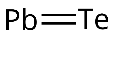
Description : We supply high-purity lead telluride (a highly important intermediate <a href="https://en.wikipedia.org/wiki/Thermoelectric_materials" rel="noopener noreferrer" target="_blank">thermoelectric material</a>)to power technological advances across global mid-temperature thermoelectric generation, mid-infrared optoelectronics, space power systems, and specialised semiconductor devices. Known to international thermoelectric fabricators as lead monotelluride and recognised across chemical supply chains as lead(II) telluride or simply lead telluride, this IV-VI narrow-bandgap semiconductor features a rock-salt cubic lattice Fm3̄m or Oh^5 with a direct bandgap of ~0.31 eV at 300 K. As the industry-standard thermoelectric material in the 400 K to 800 K temperature range, it combines high electrical conductivity with extremely low lattice thermal conductivity. Having these physical properties makes this crystal the premier choice for automotive exhaust energy harvesters, deep-space radioisotope thermoelectric generators (RTGs), mid-infrared laser diodes, and infrared sensor matrices. As global clean-tech industries transition away from unrefined alloys, processing plants are changing their sourcing methods. Companies are upgrading production lines by switching exclusively to our strictly controlled 4N (99.99%) to 5N (99.999%) purity grades to secure optimal electron movement and eliminate phase-transition material flaws. Sensor foundries partner with us as their certified global lead monotelluride supplier to protect their production runs from material failures and cross-border shipping delays. Selecting us as your trusted plumbous telluride supplier guarantees an advanced material providing uniform layer-by-layer lattice matching and structural consistency during high-speed chemical vapour deposition (CVD), molecular beam epitaxy (MBE), thermal evaporation, and spark plasma sintering (SPS). Engineering teams can verify our material metrics by downloading our batch-specific Lead Telluride COA and TDS documentation, which guarantees a precise stoichiometry ratio, strict trace-metal limits, and uniform particle sizes. Accessing our official Lead (PTe) TDS sheet ensures compliance with global standards, including European REACH registration, RoHS directives, and ISO 9001 quality rules. Partner with us as your preferred Lead Telluride (PTe) supplier to lock in raw material reserves and scale your advanced product manufacturing lines
Category : Advanced Substrates, Crystals & Quantum Materials
Sub-Category : Thermoelectric & Phase-Change Materials
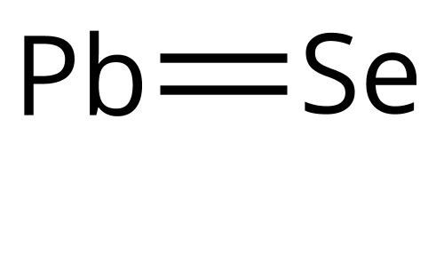
Description : Lead selenide (PbSe), or lead(II) selenide, a <a href="https://en.wikipedia.org/wiki/Selenide" rel="noopener noreferrer" target="_blank">selenide</a> of <a href="https://en.wikipedia.org/wiki/Lead" rel="noopener noreferrer" target="_blank">lead</a>, is an advanced semiconductor material. We supply high-purity Lead Selenide to fuel innovations across mid-infrared sensing, thermoelectric energy harvesting, quantum dot optoelectronics, and military thermal imaging markets worldwide. Known across international market as lead monoselenide, this IV-VI narrow-bandgap semiconductor crystal adopts a rock-salt cubic structure (Fm3m) with a direct bandgap of ~0.27 eV at room temperature. Exhibiting a positive temperature coefficient of the bandgap, high carrier mobility, and large Bohr exciton radius (46 nm), the material enables strong quantum confinement effects in colloidal nanocrystals and thin films. Having these physical characteristics make the crystal an essential component for uncooled mid-wave infrared (MWIR) photodetectors, gas absorption sensors, solid-state power generators, and lead-salt laser diodes. Global processing facilities are upgrading production lines by switching to our strictly controlled 5N (99.999%) purity grade to secure optimal electron movement and eliminate phase-transition material flaws. Sensor foundries partner with us as their certified global lead monoselenide supplier to protect their production runs from material failures and cross-border shipping delays. Choosing us as your trusted plumbous selenide supplier guarantees an advanced material providing uniform layer-by-layer lattice matching during (CVD), molecular beam epitaxy (MBE), thermal evaporation, and magnetron sputtering. Technical teams can verify our strict material metrics by downloading our batch-specific Lead Selenide COA and TDS documentation, which guarantees exact stoichiometric control, minimal trace-metal impurities, and consistent grain size distributions. Accessing our official plumbous selenide, TDS sheets ensures complete compliance with global standards, including European REACH registration, RoHS directives, and ISO 9001 quality rules. Partner with us as your preferred lead selenide supplier to lock in raw material reserves and scale your advanced manufacturing lines.
Category : Advanced Substrates, Crystals & Quantum Materials
Sub-Category : Thermoelectric & Phase-Change Materials
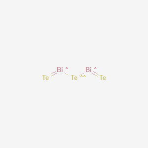
Description : Bismuth telluride is a well-studied topological insulator. Known as bismuth(III) telluride, this V-Vl binary narrow-bandgap semiconductor features a rhombohedral crystal structure (R3m) built from quintuple atomic layers (Te(1)-Bi-Te(2)-Bi-Te()) bound by weak van der Waals forces. As the industry-standard thermoelectric material near room temperature, it exhibits an exceptionally high figure of merit (ZT ~ 1.0), low lattice thermal conductivity, and Dirac-like topological surface states. Having these rare physical traits makes this unique crystal the leading choice for high-performance Peltier cooling modules, industrial waste-heat recovery generators, non-volatile phase-change memory, and infrared sensor matrices. We supply high-purity bismuth telluride (CAS No: 1304-82-1) to drive technological breakthroughs across the international thermoelectric cooling, solid-state power generation, topological insulator research, optoelectronic, and microelectronic thermal management markets. As global energy markets move away from inefficient liquid-based cooling systems, processing plants are changing their sourcing methods. Companies are upgrading their production lines by switching exclusively to our strictly controlled 3N (99.9%) to 5N (99.999%) purity grades to secure optimal electron movement and eliminate phase-transition material flaws. Thermoelectric device manufacturers partner with us as their certified global dibismuth tritelluride supplier to protect their production runs from material failures and cross-border shipping delays. Selecting us as your trusted bismuth(III) telluride supplier guarantees an advanced material that provides excellent layer-by-layer lattice matching and structural uniformity during high-speed thermal evaporation, zone melting, and magnetron sputtering deposition. Engineering teams can verify our material metrics by downloading our batch-specific Bismuth Telluride (Bi2Te3) COA and TDS documentation, which guarantees a precise stoichiometry ratio, strict trace-metal limits, and uniform particle sizes. Accessing our official Bismuth Telluride TDS sheet ensures compliance with global standards, including European REACH registration, RoHS directives, and ISO 9001 quality rules. Partner with us as your preferred Bismuth Telluride supplier to secure long-term raw material reserves and scale your advanced product manufacturing lines smoothly
Category : Advanced Substrates, Crystals & Quantum Materials
Sub-Category : Thermoelectric & Phase-Change Materials
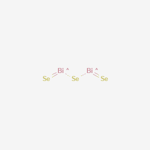
Description : We supply high-purity Bismuth Selenide (CAS No: 12068-69-8) to drive technological breakthroughs across the international thermoelectric cooling, topological insulator research, quantum computing, optoelectronic, and solid-state energy storage markets. Known across different chemical indices as dibismuth triselenide, this V-VI binary compound features a rhombohedral crystal structure (R3m) composed of quintuple layers bound by weak van der Waals interactions. As a 3D topological insulator with a bulk bandgap of ~0.3 eV, the material exhibits symmetry-protected, spin-polarised metallic surface states that allow backscattering-free electron transport. These rare electronic and thermal characteristics make this crystal the premier choice for solid-state Peltier cooling modules, high-efficiency thermoelectric power generators, spintronic logic gates, and mid-infrared photodetectors. Global technology markets are moving away from unrefined alloys, prompting processing facilities to upgrade production lines by switching exclusively to our strictly controlled 5N (99.999%) purity grade to secure optimal electron movement and eliminate phase-transition defects. Device foundries partner with us as their certified global dibismuth triselenide supplier to protect production runs from material failures and cross-border shipping delays. Selecting us as your trusted bismuth(III) selenide supplier guarantees an advanced material that provides excellent layer-by-layer lattice matching and structural uniformity during high-speed chemical vapour deposition (CVD), molecular beam epitaxy (MBE), and magnetron sputtering. Engineering teams can verify our material metrics by downloading our batch-specific Bi2Se3 COA and Selenoxobismuth TDS documentation, which guarantees a precise stoichiometry ratio, strict trace-metal limits, and uniform particle sizes. Accessing our official bismuth(III) selenide COA and TDS sheets ensures compliance with global standards, including European REACH registration, RoHS directives, and ISO 9001 quality rules. Partner with us as your preferred bismuth selenide supplier to secure long-term raw material reserves and scale your advanced product manufacturing lines.
Category : Advanced Substrates, Crystals & Quantum Materials
Sub-Category : Chalcogenide & 2D Layered Materials
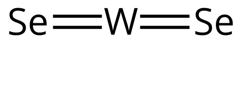
Description : We supply high-purity tungsten selenide (CAS No: 12067-46-8) to drive technological breakthroughs across the international 2D electronics, quantum semiconductor, optoelectronic, flexible photonics, and clean-energy storage markets. Known as tungsten diselenide and tungsten(IV) selenide, this layered transition metal dichalcogenide (TMD) features a hexagonal crystal structure bound by weak van der Waals forces, exhibiting a bandgap transition from an indirect 1.2 eV in bulk form to a direct 1.65 eV in monolayer architectures. Having these rare ambipolar charge-transport properties makes this unique crystal the leading choice for field-effect transistors, valleytronic logic circuits, flexible photo-detectors, and high-efficiency electrocatalytic water-splitting matrices. As global technology markets move away from rigid single-purpose materials and silicon scaling limits, processing plants are changing their sourcing methods. Companies are upgrading their production lines by switching exclusively to our strictly controlled high-purity grade to secure optimal electron movement and eliminate structural lattice flaws. Semiconductor foundries partner with us as their certified global tungsten diselenide supplier to protect their production runs from material failures and cross-border shipping delays. As global manufacturing standards shift toward high-speed chemical vapour deposition (CVD), molecular beam epitaxy (MBE), and magnetron sputtering, choosing us as your trusted tungsten(IV) selenide supplier guarantees an advanced material that provides excellent layer-by-layer lattice matching and structural uniformity. Engineering teams can easily verify our strict material metrics by downloading our batch-specific Tungsten Selenide (WSe2) COA and TDS documentation, which guarantees a precise stoichiometry ratio, strict trace-metal limits, and uniform particle sizes. Accessing our official Tungsten Selenide (WSe2) COA and TDS sheets ensures compliance with strict global standards, including European REACH registration, RoHS directives, and ISO 9001 quality rules. Partner with us as your preferred Tungsten Selenide (WSe₂) supplier to secure long-term raw material reserves and scale your advanced product manufacturing lines smoothly
Category : Advanced Substrates, Crystals & Quantum Materials
Sub-Category : Chalcogenide & 2D Layered Materials
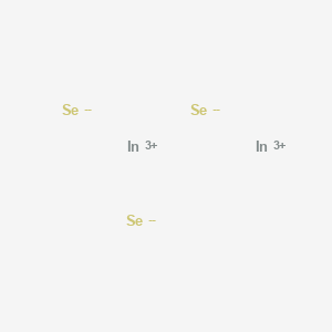
Description : We supply high-purity Indium Selenide (CAS No: 12056-07-4) to drive technological breakthroughs across the international thin-film solar, quantum semiconductor, optoelectronic, and next-generation energy storage markets. Known across different chemical indices as diindium triselenide, the mineral indium sesquiselenide features a highly versatile polymorphic crystal nature existing in “alpha, beta, gamma, and delta phases” with a direct bandgap adjusting between ~1.3 eV and 1.8 eV. Having these rare properties makes this unique crystal the leading choice for high-efficiency solar absorber formulations, fast-acting optoelectronic switches, and advanced solid-state lithium-ion battery matrices. As global energy markets move away from rigid single-purpose compounds and environmentally restricted toxic heavy metals, processing plants are changing their sourcing methods. Companies are upgrading their production lines by switching exclusively to our strictly controlled 5N (99.999%) purity grade to secure optimal electron movement and eliminate phase-transition material flaws. Solar cell manufacturers partner with us as their certified global diindium triselenide supplier to protect their production runs from material failures and cross-border shipping delays. As global manufacturing standards shift toward high-speed thermal evaporation, molecular beam epitaxy (MBE), and sputtering deposition, choosing us as your trusted indium sesquiselenide supplier guarantees an advanced material that provides excellent layer-by-layer lattice matching and structural uniformity. Engineering teams can easily verify our strict material metrics by downloading our batch-specific Indium Selenide COA and TDS documentation, which guarantees a precise stoichiometry ratio, strict trace-metal limits, and uniform particle sizes. Accessing our official Indium Selenide COA and TDS sheets ensures compliance with strict global standards, including European REACH registration, RoHS directives, and ISO 9001 quality rules. Partner with us as your preferred Indium Selenide supplier to secure long-term raw material reserves and scale your advanced product manufacturing lines smoothly. indium selenide
Category : Advanced Substrates, Crystals & Quantum Materials
Sub-Category : Chalcogenide & 2D Layered Materials
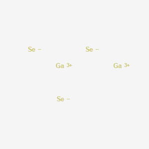
Description : We supply high-purity Gallium(III) Selenide (CAS No: 12024-24-7) to power breakthroughs in the international clean energy, heterojunction electronics, infrared optics, and phase-change memory device markets. Known across different chemical indices as digallium triselenide, the mineral gallium sesquiselenide features a defect zinc-blende crystal matrix with a wide direct bandgap of ~2.1 to 2.4 eV. These rare properties make this unique crystal the leading choice for high-efficiency thin-film solar window layers, intermediate-band solar cells, and non-volatile electrical switching storage units. As global energy markets move away from variable-grade raw materials and unstable lattice-matched interfaces, processing plants are changing their sourcing methods. Companies are upgrading their production lines by switching exclusively to our strictly controlled 5N (99.999%) purity grade to secure optimal electron movement and eliminate material flaws. International technology firms and solar cell manufacturers partner with us as their certified global digallium triselenide supplier to protect their production runs from material failures and cross-border shipping delays. As global manufacturing standards shift toward high-vacuum thermal deposition, chemical vapor transport, and sputtering methods, choosing us as your trusted gallium sesquiselenide supplier guarantees an advanced material that melts uniformly at 1020°C without leaving unwanted trace residues behind. Engineering teams can easily verify our strict material metrics by downloading our batch-specific Gallium(III) Selenide COA and TDS documentation, which guarantees a precise stoichiometry ratio, strict trace-metal limits, and uniform particle distributions. Accessing our official Gallium(III) Selenide COA and TDS sheets ensures compliance with strict global standards, including European REACH registration, RoHS directives, and ISO 9001 quality rules. Partner with us as your preferred Gallium(III) Selenide supplier to secure long-term raw material reserves and scale your advanced product manufacturing lines smoothly.
Category : Advanced Substrates, Crystals & Quantum Materials
Sub-Category : Chalcogenide & 2D Layered Materials
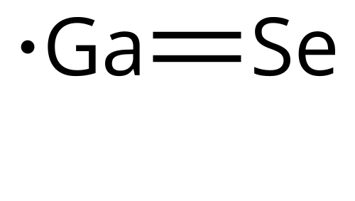
Description : We supply high-purity Gallium(II) Selenide (CAS No: 12024-11-2) to power breakthroughs in the international clean energy, terahertz (THz) optoelectronics, nonlinear optics, and flexible nanoelectronics markets. Known across different chemical indices as gallium monoselenide, and the mineral name gallium selenide features a highly anisotropic layered crystal structure with an indirect bandgap of ~2.0 eV and a direct bandgap of ~2.11 eV. These rare properties make this unique crystal the leading choice for high-efficiency frequency-doubling crystals, optical parametric oscillators, and two-dimensional (2D) layered photodetectors. As global energy and optoelectronic markets move away from bulky traditional materials and unstable active layers, processing plants are changing their sourcing methods. Companies are upgrading their production lines by switching exclusively to our strictly controlled 5N (99.999%) purity grade to secure optimal electron movement and eliminate material flaws. International technology firms and optoelectronic fabricators partner with us as their certified global gallium monoselenide supplier to protect their production runs from material failures and cross-border shipping delays. As global manufacturing standards shift toward mechanical exfoliation,(CVD), and physical vapour transport methods, choosing us as your trusted gallium selenide supplier guarantees an advanced material that maintains a hexagonal structural matrix and high structural integrity. Engineering teams can easily verify our strict material metrics by downloading our batch-specific Gallium(II) Selenide COA and TDS documentation, which guarantees a precise stoichiometry ratio, strict trace-metal limits, and uniform crystal particle sizes. Accessing our official Gallium(II) Selenide COA and TDS sheets ensures compliance with strict global standards, including European REACH registration, RoHS directives, and ISO 9001 quality rules. Partner with us as your preferred Gallium(II) Selenide supplier to secure long-term raw material reserves and scale your advanced product manufacturing lines smoothly.
Ensure globally resilient supply chains
Backed by 10+ patents and decades of experience.
Tailored support for your unique needs.
Delivering to 30+ countries.
73 products available across our advanced materials range.
Enter your personal data to create your account